UPSC Daily Current Affairs - 8th January 2026
Relevance:
GS Paper III – Economic Development, Science & Technology
Important Keywords
For Prelims:
- Design Linked Incentive (DLI) Scheme, Semiconductors, ChipIN Centre, Electronic Design Automation (EDA) Tools, Tape-out, Semiconductor IP Cores, Chips to Start-up (C2S) Programme, India Semiconductor Mission
For Mains:
- Semiconductor Ecosystem, Technological Self-Reliance, Strategic Supply Chains, Startup-led Innovation, Public Digital Infrastructure, Atmanirbhar Bharat, Design-to-Productisation Gap
Why in News?
India’s Design Linked Incentive (DLI) Scheme for Semiconductors has demonstrated strong on-ground outcomes, reflecting rapid progress in developing a domestic semiconductor design ecosystem amid rising global supply-chain vulnerabilities and strategic competition in critical technologies.
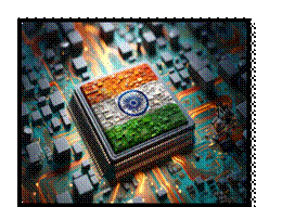
What is the Design Linked Incentive (DLI) Scheme?
The Design Linked Incentive (DLI) Scheme is a flagship initiative under the Semicon India Programme, implemented by the Ministry of Electronics and Information Technology (MeitY).
Its objective is to promote a fabless semiconductor ecosystem by providing financial incentives and advanced design infrastructure access to domestic startups, MSMEs and Indian companies engaged in chip design.
The scheme supports the entire semiconductor design lifecycle—from conceptualisation and development to deployment—covering:
- Integrated Circuits (ICs)
- Chipsets
- Systems-on-Chip (SoCs)
- Systems and IP cores
By encouraging indigenous intellectual property creation, the scheme aims to reduce import dependence, enhance domestic value addition and improve supply-chain resilience.
Eligibility under the DLI Scheme
- Startups and MSMEs are eligible for financial incentives and design infrastructure support for semiconductor product design and deployment.
- Other domestic companies are eligible for financial incentives for deployment of semiconductor designs.
Definitions:
- MSMEs: As per Ministry of MSME notification (1 June 2020)
- Startups: As per DPIIT notification (19 February 2019)
- Domestic companies: Owned by resident Indian citizens as per FDI Policy Circular, 2017 or extant norms
Financial Incentives under DLI
1. Product Design Linked Incentive
- Reimbursement of up to 50% of eligible expenditure
- Cap: ₹15 crore per application
- Applicable for semiconductor design of ICs, chipsets, SoCs, systems and IP cores
2. Deployment Linked Incentive
- Incentives of 6% to 4% of net sales turnover for five years
- Cap: ₹30 crore per application
- Minimum cumulative net sales (Years 1–5):
- ₹1 crore for startups/MSMEs
- ₹5 crore for other domestic companies
- Design must be successfully deployed in electronic products
Financial Incentives under the DLI Scheme
The Design Linked Incentive (DLI) Scheme provides two distinct but complementary financial incentives to promote indigenous semiconductor design and deployment.
1. Product Design Linked Incentive (PDLI)
This incentive supports early-stage semiconductor design and development, where costs and risks are highest.
Key Features
- Reimbursement of up to 50% of eligible expenditure incurred on semiconductor design.
- Maximum cap: ₹15 crore per application.
- Applicable to entities engaged in the design of:
- Integrated Circuits (ICs)
- Chipsets
- Systems-on-Chip (SoCs)
- Semiconductor systems and IP cores
Purpose
- Reduce entry barriers for startups and MSMEs in chip design.
- Encourage creation of indigenous intellectual property (IP).
- Strengthen India’s fabless semiconductor ecosystem.
2. Deployment Linked Incentive (DLI – Deployment Phase)
This incentive encourages commercialisation and market adoption of domestically designed chips.
Key Features
- Incentive ranging from 6% to 4% of net sales turnover.
- Incentives are provided for five years.
- Maximum cap: ₹30 crore per application.
- Minimum cumulative net sales (Years 1–5):
- ₹1 crore for startups/MSMEs
- ₹5 crore for other domestic companies
- The semiconductor design must be successfully deployed in electronic products.
Purpose
- Promote design-to-market transition.
- Ensure that supported designs achieve commercial viability.
- Link government support with real economic outcomes.
Programme Highlights & Key Achievements of DLI
Institutional Infrastructure Created
A major achievement of the DLI Scheme is the creation of shared national infrastructure for chip design:
ChipIN Centre
- Provides access to advanced Electronic Design Automation (EDA) tools
- Serves nearly 1 lakh engineers and students
- Covers 400 organisations nationwide
- Supports:
- 305 academic institutions under the Chips to Start-up (C2S) Programme
- 95 startups under the DLI Scheme
- Represents the world’s largest centralised chip design user base
Shared EDA Grid
- National platform offering high-end chip design software
- Recorded 54,03,005 cumulative usage hours (as of 2 January 2026)
- Indicates strong adoption by startups, MSMEs, and researchers across all States
Tangible Outcomes and Achievements
The enabling ecosystem has translated into measurable results:
- 10 patents filed
- 16 chip-design tape-outs completed
- 6 semiconductor chips successfully fabricated
- 1,000+ specialised engineers trained or engaged
- 140+ reusable semiconductor IP cores developed
These milestones mark India’s progress from conceptual innovation to silicon realisation.
Key Institutional Frameworks for Semiconductor Design in India
India’s semiconductor ecosystem is being built through a multi-layered institutional framework that integrates policy support, financial incentives, talent creation, and indigenous R&D, ensuring progress from chip design to productisation.
1. Ministry of Electronics and Information Technology (MeitY)
- Nodal ministry for semiconductor policy formulation and coordination.
- Anchors flagship initiatives such as the Design Linked Incentive (DLI) Scheme.
- Aims to offset structural disadvantages faced by Indian chip design firms.
- Facilitates industry–academia–government collaboration to move firms up the semiconductor value chain.
2. Semicon India Programme (SIM)
- Umbrella programme with an outlay of ₹76,000 crore.
- Provides end-to-end support across design, fabrication, and display manufacturing.
- DLI Scheme operates under SIM, ensuring continuity from design validation to manufacturing.
- Implementation supported by Centre for Development of Advanced Computing (C-DAC) as nodal agency.
3. Chips to Start-up (C2S) Programme
- National capacity-building initiative targeting academia.
- Objective: Create 85,000 industry-ready professionals at B.Tech, M.Tech, and PhD levels.
- Focuses on VLSI design, chip architecture, and system-level integration.
- Strengthens India’s long-term semiconductor talent pipeline.
4. Microprocessor Development Programme
- Implemented by C-DAC, Indian Institute of Technology Madras, and Indian Institute of Technology Bombay.
- Led to development of indigenous, open-source microprocessors such as:
- VEGA
- SHAKTI
- AJIT
- Reduces dependence on foreign IP and strengthens strategic autonomy in computing.
Success Stories of India’s Design Linked Incentive (DLI) Scheme
- Under the DLI Scheme, 24 chip-design projects have been approved in critical areas such as video surveillance, drone detection, smart energy meters, microprocessors, satellite communication, broadband and IoT SoCs.
- 95 Indian startups and companies have been provided access to industry-grade EDA tools, substantially lowering design and infrastructure costs and enabling entry into advanced chip design.
Key Beneficiary Companies and Their Contributions
- Vervesemi Microelectronics: Developing indigenous motor-control chips for BLDC motors used in household appliances, drones and electric vehicles. It holds 110+ IPs, 10 patents, and has completed pilot sampling of two chips with global customers engaged.
- InCore Semiconductors: Focused on RISC-V processor IPs, aiming to develop Dolomite, an indigenous embedded processor for smartphones and edge-AI. Its IPs are silicon-proven from 180 nm to 16 nm nodes, reducing dependence on imported CPU IP.
- Netrasemi: Designed India’s first indigenously developed AI SoC in a 12 nm node for surveillance, robotics and mobility applications, integrating in-house AI/ML accelerators.
- Aheesa Digital Innovations: Developing Vihaan, a VEGA-processor–based fiber broadband SoC enabling secure and cost-effective GPON connectivity, with reference platforms planned for 2026.
- AAGYAVISION: Working on radar-on-chip solutions for drone detection, smart infrastructure, edge computing and emerging 6G sensor networks.
- Overall, the DLI Scheme is transforming indigenous chip design into silicon-validated, market-ready products, strengthening technological self-reliance, startup innovation, and India’s position in the global semiconductor design ecosystem
Conclusion
The Design Linked Incentive (DLI) Scheme is anchoring India in the most strategic and value-intensive segment of the global semiconductor ecosystem—chip design. By reducing reliance on imported IPs, enabling silicon-validated designs, and supporting startups and MSMEs through the productisation phase, DLI is laying the foundation for technological sovereignty, supply-chain resilience, and long-term economic growth. With multiple tape-outs, patents, reusable IPs and trained talent already achieved, India is steadily emerging as a credible global hub for semiconductor design and innovation.
UPSC PYQ
Q. Which one of the following laser types is used in a laser printer?
- Dye laser
- Gas laser
- Semiconductor laser
- Excimer laser
Answer: C
Explanation:
Modern laser printers use semiconductor lasers (laser diodes) to generate a focused and scanned laser beam that forms the latent image on the photoconductor drum. Semiconductor lasers are compact, energy-efficient, low-cost, and reliable—making them ideal for printers, scanners, and barcode readers.
Other lasers serve different purposes: gas lasers (CO₂, He–Ne) for cutting or alignment, excimer lasers for UV processing, and dye lasers mainly for laboratory applications.
CARE MCQ
Q. Consider the following statements regarding Financial Incentives under the Design Linked Incentive (DLI) Scheme:
- Under the Product Design Linked Incentive, reimbursement of up to 50% of eligible expenditure is provided, subject to a cap per application.
- Under the Deployment Linked Incentive, incentives are provided as a percentage of net sales turnover for five years, subject to a maximum cap per application.
Which of the statements given above is/are correct?
- 1 only
- 2 only
- Both 1 and 2
- Neither 1 nor 2
Answer: C
Explanation:
- Statement 1 is correct: The DLI scheme provides reimbursement of up to 50% of eligible design expenditure, capped at ₹15 crore per application, for semiconductor design-related entities.
- Statement 2 is correct: The Deployment Linked Incentive offers 4%–6% of net sales turnover for five years, with a cap of ₹30 crore per application, provided the design is successfully deployed in electronic products.