
Why in News?
The Union Cabinet approved Semicon 2.0 in July 2026 to deepen India’s semiconductor capabilities across the complete chip value chain.
India also organised SEMICON India 2026 at Yashobhoomi, New Delhi, from September 17 to 19. The event, themed “Silicon to Systems: Building the Ecosystem,” brought together industry leaders, policymakers, investors, academic institutions and start-ups.
What Is a Semiconductor?
A semiconductor is a material whose ability to conduct electricity can be controlled.
Materials can broadly be understood as:
- Conductors: Materials such as copper that allow electricity to flow easily.
- Insulators: Materials that strongly resist the flow of electricity.
- Semiconductors: Materials whose electrical behaviour can be controlled according to technological requirements.
Semiconductors can switch, amplify, sense or control electrical signals. This makes them the basic building blocks of modern electronic equipment.
From Sand to a Packaged Chip
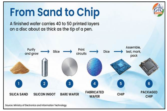
The transformation of ordinary silica sand into a semiconductor chip involves several precise stages.
Stage 1: Silicon Purification
- Silica is processed to obtain extremely pure silicon. Semiconductor manufacturing requires material with a high level of purity.
Stage 2: Ingot Formation
- The purified silicon is grown into a cylindrical silicon ingot.
Stage 3: Wafer Preparation
- The ingot is sliced into thin wafers. These wafers are polished to create smooth surfaces suitable for circuit fabrication.
Stage 4: Circuit Fabrication
The wafer undergoes hundreds of controlled operations inside a fabrication plant. Important processes include:
- Deposition: Addition of thin layers of material to the wafer
- Photolithography: Transfer of circuit patterns onto the wafer using light
- Etching: Removal of selected material to create circuit structures
- Ion implantation: Introduction of specific elements to modify electrical properties
These processes are repeated across several layers to create transistors, connections and other components.
A completed wafer may carry around 40–50 printed layers on a disc approximately as thick as the tip of a pen.
Stage 5: Dicing
- The fabricated wafer is cut into individual dies. Each functional die forms the central part of a semiconductor chip.
Stage 6: Packaging and Testing
- The die is assembled inside a protective package. Packaging allows the chip to communicate with other components of an electronic system.
- Testing determines whether the completed device meets the required performance and quality standards.
What Is a Semiconductor Node?
- A semiconductor node identifies a generation of chip-manufacturing technology.
- Earlier node labels such as 90 nanometres, 45 nanometres and 28 nanometres were closely related to specific physical measurements. Today, they mainly serve as names for different generations of manufacturing processes.
A smaller node can make it possible to place more transistors within the same chip area. This may provide:
- higher processing performance;
- lower power consumption;
- greater transistor density; and
- more features within the same chip size.
However, a smaller node does not automatically guarantee a better chip. Performance also depends on circuit design, materials, packaging and the purpose for which the chip is developed.

Advanced and Mature Nodes
- Advanced nodes support high-performance computing and leading-edge processors.
Mature nodes remain essential for:
- automobiles;
- industrial electronics;
- telecommunications;
- power systems; and
- consumer products.
India is developing capabilities ranging from established nodes towards more advanced technologies.
Applications of Semiconductors
Semiconductors are used across almost every modern sector.
Digital Technologies
- They support artificial intelligence, data centres, cloud computing, the Internet of Things and advanced communication systems.
Telecommunications
- Mobile phones, network equipment and 5G and 6G systems depend on semiconductor components.
Transport
- Automobiles, electric vehicles and autonomous vehicles require chips for control systems, sensors, batteries and safety functions.
Healthcare
- Medical equipment uses semiconductor devices for screening, diagnosis, monitoring and data processing.
Industry
- Robotics, automation, precision machinery and advanced manufacturing depend on specialised chips.
Strategic Sectors
- Defence systems, satellites, launch vehicles, unmanned aerial vehicles and naval and airborne systems require secure and reliable semiconductor supplies.
Global Semiconductor Value Chain
- The semiconductor value chain is highly specialised. No single country controls all its stages.
Different countries possess strengths in:
- chip design;
- fabrication;
- manufacturing equipment;
- specialised materials;
- memory chips;
- assembly; and
- packaging.
Taiwan, South Korea, Japan, China and the United States dominate global semiconductor manufacturing.
Taiwan accounts for:
- more than 60% of global chip production; and
- nearly 90% of advanced-chip production.
This geographical concentration creates supply risks during geopolitical tensions, industrial disruptions and other international crises.
The global semiconductor market grew at a compound annual growth rate of 6.5% between 2014 and 2024. It is projected to grow at approximately 8.5% over the next five to ten years.
Why Does India Need a Domestic Semiconductor Ecosystem?
Growing Demand
India’s semiconductor demand is projected to reach:
- $110 billion by FY2030; and
- more than $200 billion by FY2035.
The growth of electronics, telecommunications, electric mobility, artificial intelligence and digital services will further increase chip requirements.
Import Dependence
- India currently imports around 90–95% of the chips it consumes.
- Nearly $150 billion was spent on semiconductor-product imports between FY2017 and FY2025. Such imports grew at a compound annual rate of approximately 23%.
- If the trend continues, annual semiconductor imports could reach $240 billion by 2035.
Economic Security
- A domestic ecosystem can reduce the foreign-exchange burden associated with rising imports and retain a larger share of semiconductor-related economic activity within India.
National Security
- External dependence creates vulnerabilities in defence, telecommunications, space and other critical systems. Domestic capabilities can provide more reliable access to strategic chips.
Technological Competitiveness
- Chip capabilities are necessary for innovation in artificial intelligence, advanced communication, autonomous systems and high-performance computing.
Societal Development
- Domestic capacity can support wider access to modern electronic services, including affordable 5G and 6G connectivity.
India’s Existing Semiconductor Capabilities
India possesses a strong base in semiconductor design and engineering.
- The country employs nearly 20% of the global semiconductor chip-design workforce.
- It hosts approximately 7% of the world’s semiconductor-domain Global Capability Centres.
- More than one lakh engineers have received access to advanced chip-design tools.
- Academic institutions and start-ups are increasingly participating in chip development.
The Semiconductor Laboratory at Mohali has provided an institutional foundation for developing specialised chips required for strategic purposes.
Semiconductors in India’s Strategic Missions
The Semiconductor Laboratory develops flight-grade and radiation-resistant devices capable of functioning under extreme space conditions.
Its important contributions include:
- an Indian-made camera chip used in the Chandrayaan-3 lander;
- the Vikram processor used in satellite launch vehicles and rockets;
- radiation-hardened analogue-to-digital converter chips used in Aditya-L1; and
- flight-grade chips for satellites and launch vehicles.
These applications show India’s existing capacity to design semiconductor components for specialised national missions.
Semicon 1.0: Laying the Foundation
The Government approved Semicon 1.0 in December 2021 with an outlay of ₹76,000 crore.
The programme focused on creating the initial foundation for semiconductor and display manufacturing.
Major Components
- Scheme for setting up semiconductor fabs
- Scheme for setting up display fabs
- Support for compound semiconductors
- Support for silicon photonics and sensor facilities
- Incentives for ATMP and OSAT plants
- Design Linked Incentive Scheme
Major Achievements
Manufacturing Units
Twelve semiconductor manufacturing units were approved with a combined investment exceeding ₹1.64 lakh crore.
They include:
- one silicon fab;
- one silicon-carbide fab;
- one Gallium Nitride Micro-LED Display Fab; and
- nine ATMP/OSAT units.
The units are located in Gujarat, Assam, Uttar Pradesh, Odisha, Punjab and Andhra Pradesh. Five have commenced commercial production.
Chip Design
Twenty-four chip-design projects, valued at approximately ₹900 crore, were approved.
Advanced design tools were made available to over one lakh engineers from 500 organisations, including:
- 400 academic institutions; and
- 100 start-ups.
These organisations developed more than 300 chip designs.
Semicon 2.0: Building the Complete Ecosystem
Semicon 2.0 was approved with an outlay of ₹1,27,500 crore.
The programme seeks to expand India’s capabilities beyond fabs and packaging by developing all major parts of the chip value chain.
Six Pillars of Semicon 2.0
Design
- Development of strategic and commercial chips for Indian and international markets.
Machines and Materials
- Creation of capabilities in manufacturing equipment, specialised gases, chemicals and other essential materials.
Fabrication Facilities
- Establishment of additional silicon, compound-semiconductor and display facilities.
Packaging
- Expansion of conventional and advanced ATMP and OSAT capabilities.
Research
- Support for advanced nodes, emerging technologies and domestic semiconductor innovation.
Talent
Development of engineers, technicians, operators and researchers required by the semiconductor industry.
Semicon 1.0 and Semicon 2.0
| Semicon 1.0 | Semicon 2.0 |
| Established the initial ecosystem | Seeks to complete the value chain |
| Focused mainly on fabs and packaging | Adds materials, machines, research and talent |
| Expanded manufacturing and design | Deepens long-term technological capability |
| Created foundational capacity | Targets a globally competitive ecosystem |
Supporting Government Policies
National Policy on Electronics, 2019
It established the broad framework for Electronics System Design and Manufacturing, including chipsets and other electronic components.
SPECS, 2020
- The Scheme for Promotion of Manufacturing of Electronic Components and Semiconductors provides capital-expenditure-linked incentives for components, sub-assemblies and semiconductor manufacturing.
Modified Electronics Manufacturing Clusters Scheme, 2020
- EMC 2.0 supports common infrastructure, world-class facilities and plug-and-play manufacturing environments.
PLI for Large-Scale Electronics Manufacturing, 2020
- It promotes domestic manufacturing and investment in mobile phones and electronic components.
PLI 2.0 for IT Hardware, 2023
- It supports the domestic production of laptops, tablets, all-in-one computers and servers.
Electronics Components Manufacturing Scheme, 2025
- The scheme promotes component manufacturing and higher domestic value addition. Its outlay was enhanced to ₹40,000 crore in the 2026–27 Budget.
Mobile Phone Manufacturing Scheme, 2026
- It seeks to deepen the mobile-manufacturing supply chain, increase domestic value addition and support Indian mobile brands.
Research, Development and Innovation Scheme
- It supports eligible semiconductor research projects under Semicon 2.0.
Foreign Direct Investment
- India permits 100% FDI in electronics manufacturing, facilitating global investment, technological collaboration and value-chain integration.
International Semiconductor Partnerships
India has established semiconductor cooperation with:
- the United States;
- Japan;
- the European Union;
- Singapore; and
- the Netherlands.
During the German Chancellor’s visit in January 2026, India and Germany signed a Joint Declaration of Intent on a semiconductor ecosystem partnership.
- India also joined Pax Silica during the India AI Impact Summit in February 2026.
- These partnerships complement domestic capacity by supporting technology cooperation, investment and integration with global value chains.
Significance for India
Supply-Chain Resilience
Domestic capabilities can reduce India’s exposure to disruptions in geographically concentrated production networks.
Strategic Autonomy
Reliable access to domestically designed and manufactured chips can strengthen critical systems in space, defence, telecommunications and digital infrastructure.
Domestic Value Addition
Manufacturing more stages of the chip within India can retain investment, production and technical knowledge within the national economy.
High-Value Employment
Research, design, fabrication, equipment manufacturing and packaging can generate specialised employment for engineers, researchers, operators and technicians.
Global Competitiveness
India can combine its large chip-design workforce with expanding manufacturing capacity and trusted international partnerships.
Major Challenges
- Semiconductor manufacturing is among the world’s most complex industrial activities.
- India’s domestic fabrication capacity remains at an early stage.
- Advanced production is concentrated in a small number of countries.
- The complete ecosystem requires simultaneous progress in design, materials, machinery, fabs, packaging, research and talent.
- Manufacturing requires a high degree of precision and sustained technological development.
- The sector needs patience and consistent long-term policy support.
Conclusion
India’s semiconductor journey is progressing from design strength and strategic applications towards complete domestic manufacturing. Semicon 1.0 established the initial foundation, while Semicon 2.0 expands the mission to equipment, materials, research and talent. Long-term implementation can reduce import dependence, strengthen technological security and position India as a trusted participant in the global semiconductor ecosystem.